
Get in Touch
Your Trusted Manufacturer of Laptops & Tablets

WhatsApp Us Directly
+86 13923410269
Email Us
Get in Touch
Your Trusted Manufacturer of Laptops & Tablets

Let me give you the short answer upfront: A full private-mold OEM customization for an AI edge computer typically takes 4 to 6 months from initial concept to mass production. If you opt for an off-the-shelf public mold with just logo printing, that timeline shrinks to 45–60 days.
But if any manufacturer promises you a 'brand-new private mold in 30 days' — here's my honest take: walk away. Fast.
Why does it take this long? What exactly are you and your supplier grinding through during those 4–6 months? Why do some projects stall out at the 3-month mark while others sail through to delivery? Today, I'm breaking down the entire private mold development process for AI edge computers — layer by layer, stage by stage. There are far more moving parts than most buyers initially realize.
Let's clear this up first.
If you browse any e-commerce platform for 'AI edge computing boxes,' you'll see dozens of black metal enclosures that look nearly identical. If all you need is a working inference machine, buying an off-the-shelf unit is fine. But if you're pursuing OEM customization, you're after something far more significant than a logo swap.
AI edge computer OEM customization typically spans four distinct layers:
Layer 1: Industrial Design (ID) — Changing colors, silk-screening, and packaging graphics. This is the shallowest level of customization.
Layer 2: Mechanical Design (MD) — Repositioning I/O ports, redesigning ventilation slots, and relocating motherboard standoffs. This requires mold modifications.
Layer 3: Hardware / Mainboard — Swapping core chips (e.g., from Rockchip RK3588 to Sophon BM1684), adding/removing memory modules, adjusting storage configurations (eMMC to SSD), and changing network interfaces (dual Gigabit to 10GbE). This is where the actual compute power lives.
Layer 4: Firmware & BSP — Tailoring the Linux/Android kernel, preloading NPU drivers, and flashing specific AI inference frameworks (like Tengine or ONNX Runtime). This is the soul that makes the hardware actually work.
If your customization stops at Layer 1, we're talking weeks. But if you're touching Layers 3 and 4, that 4-to-6-month industry standard is non-negotiable. Each layer requires its own physical validation and software debugging cycle — and there's no shortcut around physics.
A 'private mold' means you're paying for the tooling — the molds that produce your unique enclosure. Nobody else gets to use them. The fundamental difference from a public mold is this: a public mold is a pre-furnished apartment you move into; a private mold is buying land and building your own foundation from scratch.
Here's the 6-stage breakdown, mapped against a realistic timeline.
Stage 1: Requirements Definition & Platform Selection (2–4 Weeks)
This is the most underestimated phase of the entire project. Too many buyers come in saying, 'I need a high-performance AI box' — but when asked the critical questions, they draw a blank:
The deliverable from this stage is a Product Requirement Specification (PRS) document. Your ODM partner needs 2–4 weeks to perform hardware selection and feasibility studies — and here's the kicker: component lead times are a growing concern. With AI chips in constant shortage, picking a chip with a 30-week lead time will kill your schedule before you even start.
Pro tip for overseas buyers: When evaluating potential suppliers, ask for their preferred chipset portfolio. Suppliers with established relationships with Rockchip, Amlogic, and NVIDIA often have better access to allocation — and that directly impacts your timeline.
Stage 2: ID Design & MD Engineering (3–5 Weeks)
ID is the 'render' — what the box looks like. MD is the 'blueprint' — how the mainboard fits inside, how heat gets dissipated, how antennas are positioned without signal interference.
Here's where things get messy. Your ID designer creates a stunning, ultra-slim, fanless, fully sealed minimalist metal enclosure. It looks beautiful. Then your MD engineer takes one look and says, 'This can't dissipate 15W from the NPU.' Back to the drawing board. Add fins. Add vents. The ID designer hates it. The MD engineer says it's either this or thermal throttling.
This back-and-forth is completely normal — but it's also why a 3-week engineering phase can easily stretch to 5. The smart move: work with an ODM where ID and MD teams collaborate in parallel from day one, rather than sequentially.
Stage 3: Tooling & T0 Trial Molding (25–35 Days)
This is the longest and least predictable phase in the entire private mold process.
Tooling falls into two categories: injection molds (plastic enclosures) and die-cast molds (aluminum enclosures). A complex aluminum die-cast mold alone takes roughly 30 days to cut. T0 trial molding is the first time the mold goes onto the injection machine to produce a handful of 'prototype' units for verification.
Here's the reality: T0 samples almost never come out perfect. You'll see sink marks, flash (burrs), ejector-pin marks, and dimensional tolerances that prevent the mainboard from fitting. This is expected. The mold goes back for rework — that's T1. Then another round — T2. And so on, until dimensional inspection passes.
Here's a hidden cost most buyers don't anticipate: Mold rework itself is usually included in the tooling fee. But each trial run ties up an injection machine — and if the factory's machine schedule is packed, you wait. This is exactly why your supplier keeps pushing you to 'approve the samples quickly' — your mold is occupying production capacity they could use for other clients.
For overseas buyers: If your volume is under 1,000 units, the per-unit tooling amortization can be brutal. Always ask for a tooling cost breakdown and consider whether a public mold with custom painting might give you 80% of the differentiation at 20% of the tooling investment.
Stage 4: PCB Fabrication & SMT Assembly (15–20 Days)
While the enclosure is being tooled, the mainboard PCB design and fabrication run in parallel. After PCB layout is finalized, it goes to the board house for fabrication — standard lead time is 7–10 days. Bare boards then go through SMT assembly: soldering resistors, capacitors, and mounting the CPU/NPU chips. You'll typically get 3–5 engineering prototypes out of this stage within 20 days.
The single biggest risk here? Component availability. If you didn't secure chip inventory upfront, your Rockchip or NVIDIA chips could have 12–16 week lead times. Your mold could be ready in 30 days — but you'll have nothing to put inside it.
Critical advice for procurement teams: Before signing any contract, ask your supplier for a BOM (Bill of Materials) lead-time assessment. Identify all long-lead components and either place advance orders or secure allocation commitments.
Stage 5: EVT, DVT & Comprehensive Testing (3–4 Weeks)
Once the engineering samples are assembled, you enter the most compressed-but-critical phase: validation testing. This is the stage that inexperienced buyers try to shortcut — and it's precisely the stage where you cannot afford to cut corners.
Here's what the test matrix looks like:
If any of these tests fail, you'll need PCB layout modifications or structural tweaks — followed by another prototype run (DVT — Design Verification Test). Then another validation cycle (PVT — Production Verification Test). This is exactly why a 4-month project becomes a 6-month project. Most of the slippage happens in these 'test-fail-fix-retest' loops.
For product managers: Build at least 2–3 weeks of buffer into your project plan specifically for this phase. Don't assume first-pass yield. Assume you'll need at least one iteration — and be pleasantly surprised if you don't.
Stage 6: Certifications & Pilot Production (3–4 Weeks)
After PVT passes, you need mandatory regulatory certifications: FCC (US), CE (Europe), and UKCA (UK). Certification typically takes 2–3 weeks, with costs ranging from $5,000 to $20,000+ depending on complexity and the number of wireless radios (WiFi, Bluetooth, 4G/5G) on board.
Once certified, you move to pilot production — typically 50–200 units to validate assembly line processes and confirm yield rates. Only after pilot production passes the yield gate (industry standard: >98% first-pass yield) do you proceed to full-scale mass production.
The timeline above assumes everything goes smoothly. In reality, these three pitfalls are responsible for most delays — and they're entirely avoidable if you know what to watch for.
Pitfall #1: Midstream Chipset Changes. You're 2 months into tooling, and your chosen AI chip just spiked 3x in price. You want to switch to an alternative. Here's the problem: the mainboard layout changes. The thermal solution changes. The I/O port positions on the mold may change. You've just invalidated the previous 2 months of work. This is the single most expensive mistake you can make.
Prevention: Lock your chipset selection before tooling begins. Include a 'chipset contingency plan' in your contract — if the primary chip becomes unavailable, what's the approved secondary option with minimal re-engineering?
Pitfall #2: Ignoring Assembly Tolerances in Mechanical Design. This is surprisingly common. The ID team pushes the enclosure design to the absolute limit — leaving only 0.2mm of clearance between the mainboard and the housing. T0 trial molding reveals the enclosure warped by exactly that 0.2mm. Now the mainboard doesn't fit. Rework: 7 days. Re-trial: 10 days. Two weeks gone, just like that.
Prevention: Insist on a tolerance stack-up analysis before tooling starts. Add 0.3–0.5mm of additional clearance to every critical fit. That extra margin is insurance against the inevitable warpage of real-world injection molding.
Pitfall #3: Thermal Failure During Validation. Your edge AI box runs a 15W NPU. In a fanless design, that heat has to conduct through thermal pads into the entire metal enclosure as a heatsink. During thermal testing, the enclosure surface hits 85°C — too hot to touch, failing safety regulations. The fix? Redesign the thermal path. Add more fins. Sometimes, re-cut the mold to increase surface area — which is both expensive and time-consuming.
Prevention: Run thermal simulation during the MD phase — before any tooling is cut. Good ODMs do this as standard practice. If your supplier doesn't offer thermal simulation, that's a red flag.
Here's my straightforward take for overseas buyers: If this is your first AI edge product, launch with a public mold to validate the market — then go private mold for differentiation.
Public mold advantages: Fast (45-day delivery), low entry cost (no tooling fee), proven thermal and mechanical designs. Disadvantages: Everyone has access to the same enclosure. Your differentiation comes down to price and service — not product uniqueness.
Private mold advantages: Exclusive industrial design, tailored I/O placement, custom thermal solutions optimized for your specific use case. Disadvantages: High upfront investment ($10,000–$30,000+ for tooling), longer timeline (4–6 months).
The break-even rule of thumb: Go private mold when you've validated at least 1,000–2,000 units of demand through a public mold, and your unit price exceeds $400. If your unit price is under $150, you'd need to sell 5,000+ units just to recover tooling costs — at which point the math may still favor public mold with custom finishing.
Take these three steps before signing any contract — they'll shave at least 3 weeks off your project timeline.
①Evaluate the Software Ecosystem Before the Hardware. AI edge chips all boast impressive TOPS numbers. But what matters more is toolchain maturity — how easy is it to convert your model (say, YOLOv8) to run on that NPU? Some chips have terrible SDKs and buggy quantization tools. Your algorithm team could spend 3 weeks fighting a toolchain issue that a competing platform solves in 2 days. Always ask for a live model conversion demo before committing.
②Insist on Mechanical Stack-Up Drawings, Not Just Renders. Renderings are beautiful. They sell the vision. But they don't show you the internal reality: where the thermal pad sits, how much clearance the antenna has, whether the heatsink is tall enough for your power budget. Review the mechanical stacking drawing with your own hardware engineer before tooling starts. If that drawing shows a 3mm heatsink on an 8W NPU, you already know thermal testing will fail.
③Put Clear Acceptance Criteria in the Contract. Vague milestones are the enemy of on-time delivery. Get specific. Put it in writing:
With clear penalties tied to missed milestones (or performance bonuses for early delivery), your supplier's production planning team will prioritize your project over others in their pipeline.
Industry-Specific Solutions
Latest Blog

How to Choose an Edge Computing Box Manufacturer: ODM/OEM Guide
Learn how to evaluate edge computing box manufacturers. Compare source factories, ODM/OEM models, MOQ, certifications, and customization to find the right partner.

How to Choose an AI Mini PC in 2026: NPU & Memory Buying Guide
A practical guide to choosing an AI mini PC in 2026. Learn how to match NPU TOPS, memory capacity, and bandwidth to your workload, avoid common pitfalls, and pick the right configuration.
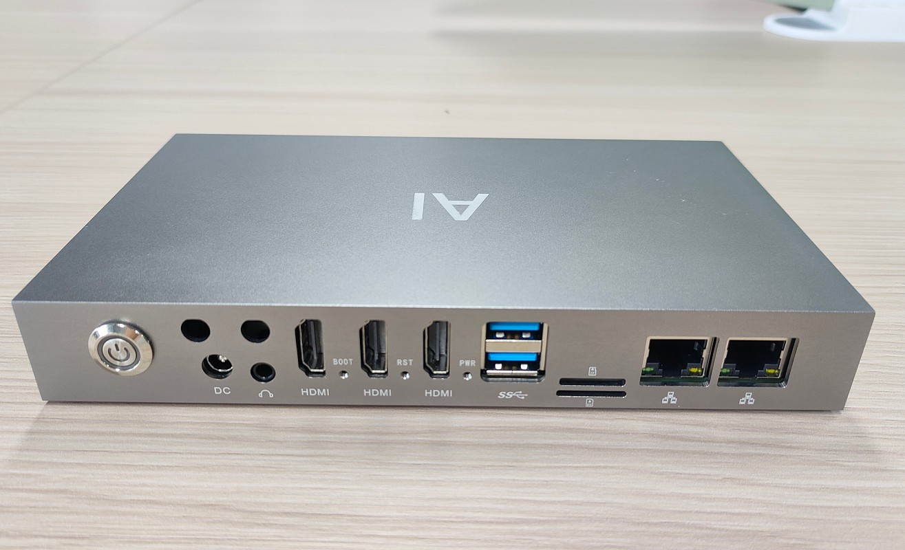
How to Partner with an Edge Box Manufacturer
Complete OEM/ODM process for edge computing boxes – from requirements and factory vetting to sample sign‑off, pilot runs, and bulk delivery. Includes contract tips and IP protection.
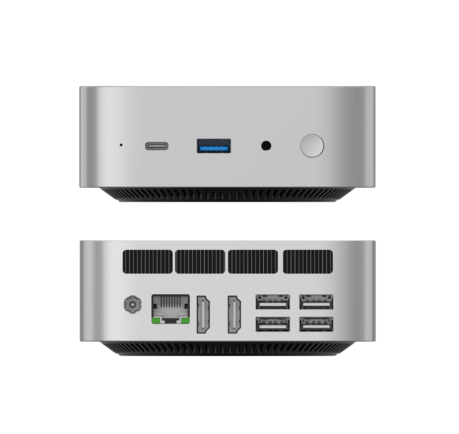
What Is an Edge Box? Compare with PC, AI Mini PC & Edge Server
What is an edge box and how does it differ from a regular PC, AI mini PC, or edge server? This guide explains edge box features, use cases, and selection criteria for AI inference at the edge.
Adreamer

© 2012-2025 Copyright Shenzhen Adreamer Technology Co., Ltd.粤ICP备18115621号-2
Contact Adreamer Today for Your Custom Solution & Quote!
© 2012-2025 Copyright Shenzhen Adreamer Technology Co., Ltd.粤ICP备18115621号-2