
Get in Touch
Your Trusted Manufacturer of Laptops & Tablets
WhatsApp Us Directly
+86 13923410269
Email Us
Get in Touch
Your Trusted Manufacturer of Laptops & Tablets

From concept to mass production: a deep dive into the full-cycle process of private‑mold AI box customization—covering ID design, mechanical engineering, tooling, thermal validation, certification, and pilot runs—to help you plan your project timeline with confidence.
You have a vision for an edge AI product—perhaps a smart retail analytics terminal, an industrial quality‑inspection box, or a security edge node. You want it to have a distinctive industrial design, just‑right computing power, and your own brand identity—not another off‑the‑shelf generic enclosure.
So you need a custom‑mold AI box—a completely new enclosure and motherboard tailored to your exact requirements.
But the first question hits you: How long will this take? Three months? Six months? A year?
To be blunt, many suppliers are vague on this—either quoting an overly optimistic timeline to win the order, or padding it excessively to avoid blame. This guide pulls back the curtain, giving you a procurement‑friendly, phase‑by‑phase breakdown of the entire OEM customization journey. You will learn the exact duration of each stage, the critical decision points, and how to plan your project schedule realistically—so you can avoid being trapped by either unrealistic promises or over‑cautious estimates.
Before we dive into the details, here is a clear, benchmarked answer.
| Customization Type | Typical Timeline | Best For |
|---|---|---|
| Standard product with logo change (light) | 4–6 weeks | Only logo silkscreen, packaging, and pre‑loaded software; no hardware changes |
| Modified standard mold (medium) | 8–12 weeks | Altering top cover, I/O panel, color, or surface finish on an existing chassis |
| Semi‑custom (mid‑high) | 14–18 weeks | New tooling for some parts (e.g., top/bottom covers), adjusted PCB layout, re‑routed I/O |
| Full private mold (deep) | 20–28 weeks (5–7 months) | Entirely new ID design, all‑new tooling, brand‑new motherboard, custom thermal solution |
Conclusion: If you need a fully private‑mold AI box—inside and out—plan for 5 to 7 months. This is the industry baseline, not a supplier’s “special case.”
Of course, these are industry averages. Actual execution varies with complexity and factory load. Later sections will show you how to compress the timeline through smart preparation.
To understand the timeline, you first need to grasp the difference between standard (off‑the‑shelf) molds and private molds.
| Aspect | Standard Mold (ODM Catalog) | Private Mold (Full Custom) |
|---|---|---|
| Appearance | Factory‑standard enclosure | Brand‑new industrial design, exclusive to you |
| Tooling | Existing mold; no tooling fee | New injection‑molding or die‑casting tooling; tooling cost applies |
| Motherboard | Fixed reference design | Custom layout, I/O placement, and size |
| Branding | No logo or simple silkscreen | Custom logo, boot screen, packaging, and complete branding |
| Exclusivity | Anyone can buy the same design | Your design belongs to you (usually with a mold agreement) |
| Minimum Order Quantity | 100–500 units | Typically 1,000–3,000 units |
“Tooling development” is the longest single phase. For a mini‑PC or small‑form‑factor box, injection‑mold tooling—from design review to first shots to production‑ready—takes 4–8 weeks on its own. Add mechanical design, prototype iterations, and engineering adjustments, and you can see why the total stretches to several months.
Tip: Some suppliers offer a “shared private mold” model—you pay the tooling cost, the mold belongs to you, but the supplier may sell the same enclosure to non‑competing customers (different regions or industries) to share the cost. If you want full exclusivity, expect higher tooling fees.
This is the foundation of the entire project—and the most overlooked. Unclear requirements will cause endless rework in later phases.
What you need to define:
Key advice: Prepare a detailed Product Requirement Document (PRD) before engaging suppliers. This can compress the definition phase from 4 weeks down to 2, and it prevents later rework.
ID transforms your brand identity and functional needs into a 3D visual concept.
Activities:
Deliverables: 3D renderings, CMF specification document.
Potential pitfall: Endless design iterations due to subjective preferences vs. engineering feasibility. Agree on a maximum number of revision rounds in the contract (e.g., 3 free rounds, extra charged) to keep the phase on track.
ME translates the ID into manufacturable engineering drawings.
Activities:
Deliverables: 3D mechanical files (STP/IGS), 2D engineering drawings.
Prototyping uses CNC machining or 3D printing to produce 1–3 physical shell samples to verify fit and assembly.
What is verified:
Tip: Prototyping is the “pay a little to avoid a big loss” step. A few thousand dollars for prototypes can prevent discovering interference after the mold is cut—which would cost tens of thousands and many weeks to fix. Always assemble with a real or dummy PCB of the correct size.
EVT uses prototype shells + engineering‑sample motherboards to verify basic functionality.
Tests:
Deliverables: EVT test report, issue log.
DVT is the comprehensive engineering validation before tooling is finalised. At this stage, shells are from trial shots (not prototypes), and the motherboard is the final engineering version.
Tests:
Critical decision point: Once DVT passes, the design is frozen—no more changes to appearance or dimensions. Any modifications after this point require mold rework and delay the project significantly.
PVT uses production‑intent tooling and formal assembly processes to build 50–200 units.
Objectives:
Deliverables: PVT samples (available for customer testing), PVT test report.
Tip: PVT units should be identical to mass‑production units—same mold, same line, same materials. For orders above 500 units, conduct real‑environment testing with these samples—typically 2 weeks suffice. If major yield or performance issues arise, you may need to loop back to DVT, adding 4–8 weeks.
Once PVT is approved, full‑scale production begins.
Activities:
Production capacity reference: A typical line produces 500–1,000 units per day, depending on assembly complexity and test duration.
Beyond the standard process, these factors often add significant lead time. Plan for them upfront.
| Platform | Supply Stability | Impact on Timeline |
|---|---|---|
| Rockchip RK3588 | Stable | Baseline |
| Intel Core Ultra | New models may have tight supply | +2–4 weeks |
| NVIDIA Jetson Orin | Industrial‑grade variants may be constrained | +4–8 weeks |
| Qualcomm/MTK | BSP maturity varies | +2–4 weeks |
| Target Markets | Typical Duration | Can Be Parallelised? |
|---|---|---|
| China only (CCC) | 4–6 weeks | Yes, with DVT |
| EU (CE + RoHS) | 6–8 weeks | Yes |
| USA (FCC) | 4–6 weeks | Yes |
| Multiple (CE+FCC+UKCA+CCC) | 10–12 weeks | Plan as a separate track |
If any certification test fails, add 2–4 weeks for fixes and re‑test.
Tip: Run certification tests in parallel with DVT to avoid making certification the critical path.
Place orders for critical components (SoC, RAM, storage) as soon as the project starts. When DVT passes, materials are already in stock and mass production can begin immediately—saving 4–8 weeks of procurement tim.
Do not wait for one phase to fully finish before starting the next. For example:
Some ODMs offer pre‑validated reference designs for AI platforms (RK3588, Jetson, etc.). Using these can reduce motherboard development from 8 weeks to just 3–4 weeks—you only need to adjust I/O and enclosure.
Contractually cap the number of free revision rounds (e.g., 3 rounds for ID, 3 for ME). Each extra round adds 1–2 weeks on average.
Add 2–4 weeks of buffer to your project schedule for unexpected engineering challenges (thermal rework, ESD fixes). This is a sign of professional project management, not procrastination.
Selecting the right supplier is the most critical factor in keeping your timeline realistic. Here is a quick evaluation checklist.
| Evaluation Dimension | What to Check |
|---|---|
| ID/ME capability | Do they have successful private‑mold cases? Can you see physical samples? |
| Motherboard experience | Have they delivered AI platforms (RK3588/Jetson/Intel) before? |
| Tooling resources | Does their mould partner have available capacity? What is the typical trial‑shot lead time? |
| Certification track record | Have they passed CE/FCC/CCC as a complete system? Do they do in‑house pre‑testing? |
| FAE support | Do they have local field application engineers? What is the response mechanism? |
Tip: Do not choose solely on price. An inexperienced but cheap supplier may get stuck in DVT for 3 months—the time cost will far outweigh any unit‑cost savings.
| Phase | Key Activities | Typical Duration | Critical Decision Point |
|---|---|---|---|
| Requirement Definition | PRD writing and review | 2–4 weeks (can be front‑loaded) | SoC selection, I/O definition |
| ID Design | Appearance & CMF design | 3–5 weeks | Design freeze |
| Mechanical Design | PCB stacking & engineering drawings | 3–4 weeks | DFM sign‑off |
| Prototyping | CNC/3D‑printed samples | 1–2 weeks | Fit confirmation |
| EVT | Functional verification | 2–3 weeks | Motherboard feature freeze |
| DVT | Thermal/ESD/reliability validation | 3–4 weeks | Structure freeze |
| PVT | Pilot run & testing | 2–3 weeks | Yield approval |
| Mass Production | Volume manufacturing & shipping | 4–8 weeks | Final delivery |
| Full Private Mold Total | ~20–28 weeks (5–7 months) |
OEM customisation of an AI box is not a “order today, ship next month” affair. It is a systematic engineering project involving industrial design, mechanical engineering, hardware development, tooling, and certification.
5–7 months sounds long—but it is the industry standard. What truly derails projects is rarely the process itself; it is:
With proper preparation, a trusted partner, and parallel working, 5 months is achievable. Without these, even a year may be wasted on endless rework.
One final piece of advice: Before you start, ask yourself: “Is this AI box a core product for our next 2–3 years, or a one‑off project device?”
We hope this guide helps you map out a realistic schedule and turn your AI hardware vision into reality—on time and on budget.
Industry-Specific Solutions
Latest Blog
N100 vs N95 Mini PC Performance Comparison
Compare Intel N100 vs N95 mini PCs. See CPU, iGPU, TDP, power draw, gaming, and NAS performance—plus clear buying advice for office, soft router, and light gaming.
RK3588 vs RK3588S: Key Differences for Edge Computing Boards
Compare RK3588 and RK3588S for edge computing. Learn PCIe, SATA, Ethernet, and MIPI interface differences to choose the right board for your project’s expansion needs.
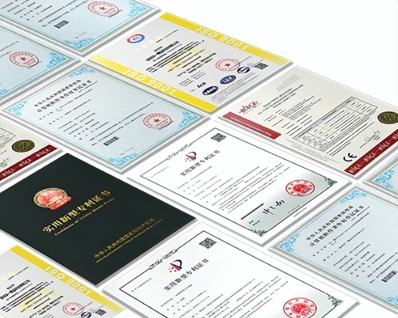
AI Compute Box Bulk Procurement: 3C, CE, FCC Certification Guide
Learn the key certification requirements for bulk buying AI compute boxes. Covers 3C, CE, FCC compliance, common pitfalls, and how to verify certificates to avoid legal risks.

RK3588 vs N100: Which Is Better for Local LLM Deployment?
Compare RK3588 and N100 for running local LLMs. See real-world token speeds, power, memory, software support, and which chip fits your AI workload.
Adreamer

© 2012-2025 Copyright Shenzhen Adreamer Technology Co., Ltd.粤ICP备18115621号-2
Contact Adreamer Today for Your Custom Solution & Quote!
© 2012-2025 Copyright Shenzhen Adreamer Technology Co., Ltd.粤ICP备18115621号-2